Note: Stereo and bridged amplifier PCBs are available for this project.
The TDA2003 is a low cost audio chip amplifier that can put out some really nice sounds. It’s typically used for car audio amplifiers, but it also works great as a bedroom amp or anywhere else you need good audio without tons of power.

In this tutorial, I’ll show you how to build two different amplifiers with the TDA2003. The first is a stereo amplifier that will output 7 Watts per channel. The second is a bridged amplifier that can output 14 Watts per channel.
If you don’t already have it, I recommend downloading and reading the datasheet for the TDA2003. Actually there are two different datasheets. The ST Microelectronics datasheet is the original manufacturer’s datasheet, but the Contek datasheet has additional schematics for the bridged amplifier:
![]() ST Microelectronics TDA2003 Datasheet
ST Microelectronics TDA2003 Datasheet
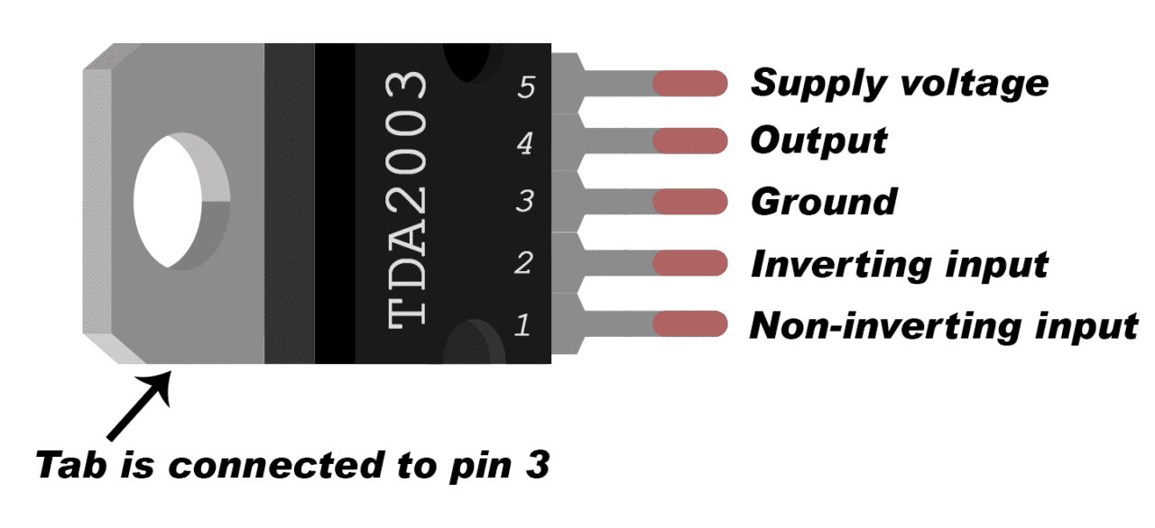
Here’s a diagram of the TDA2003 pinout:
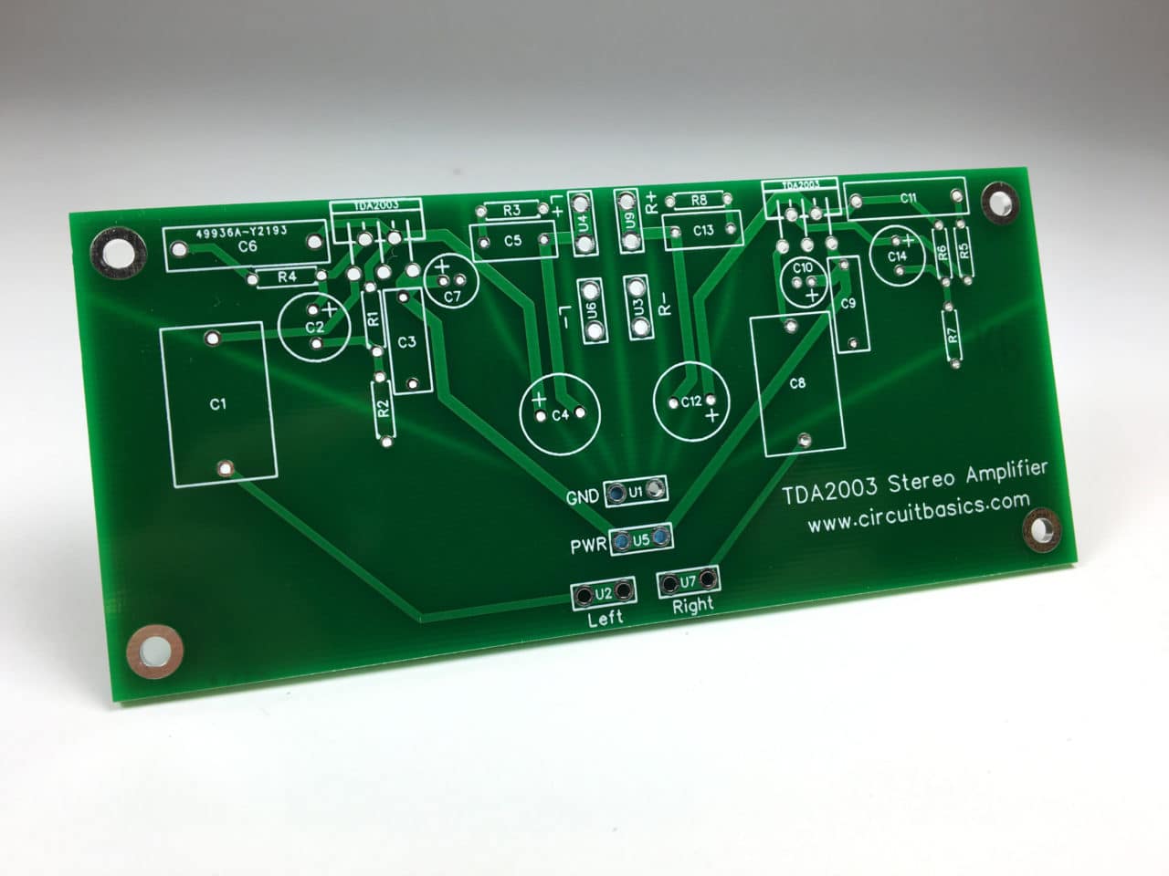
TDA2003 Stereo Amplifier
This stereo amplifier will output about 7 Watts per channel into 2 Ω speakers with a 12 V power supply, but more power can be had with a larger power supply voltage.
Watch a quick video where I explain some of the design principles and wire it up so you can hear how it sounds:
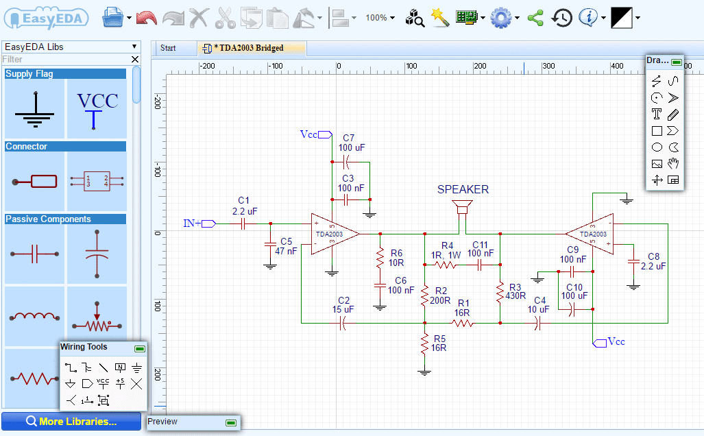
Stereo Amplifier Schematic
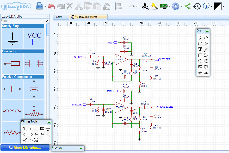
This schematic is similar to the one in the datasheet, but it has a couple other parts to help reduce noise:
- Capacitors C15 and C17: Reduce hum caused by radio frequency interference.
- Resistors R9 and R10: Prevent a loud buzzing sound when no source is connected.
Setting the Gain
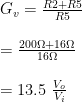
The left channel gain is set by resistors R1 and R2, while the right channel gain is set by R6 and R7. The gain is set to 101 Vo/Vi on both channels, but you can change it by using different values for R1 and R6. Use the formula below to find the resistance values for your desired gain:
Left channel:

Right channel:

The voltage gain can be thought of as the amplification factor, or how many times the input signal is amplified.
You can calculate the gain you’ll get with a particular set of resistors with this formula:
Left channel:

Right channel:

It’s important to use low tolerance resistors for R1, R2, R6, and R7. If their resistances aren’t precise, the gain will be different on each channel and make one side louder than the other. Your best bet will be 0.1% tolerance metal film resistors.
Setting the Bandwidth
The amplifier’s bandwidth determines which frequencies are amplified and which are ignored. The TDA2003 has a low pass resistor-capacitor (RC) filter at the output that filters out all frequencies above a certain cutoff frequency (Fc). All frequencies below the cutoff frequency are passed on to the speakers.
The low pass filter is formed by C6 and R4 in the left channel and C11 and R5 in the right channel. You can calculate the cutoff frequency with this equation:

For example, this amplifier has C6 and C11 at 39 nF; and R4 and R5 at 39 Ω. The cutoff frequency is:
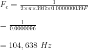
So all frequencies above 104.6 kHz are filtered out, and frequencies below 104 kHz are output to the speakers. If you want to experiment with higher or lower cutoff frequencies, the equation above can be rearranged to solve for a resistor or capacitor value depending on your desired cutoff frequency.
Power Supply Decoupling Capacitors
Capacitors C7 and C3 in the left channel and C9 and C10 in the right channel are the power supply decoupling capacitors. They provide a quick and lasting supply of current to the chip during periods of heavy output and also filter electromagnetic interference in the power supply. You can use other values than what is shown in the schematic, but each chip should have at least one small value capacitor between 1 µF and 100 nF, and one larger value capacitor greater than about 47 µF.
Bass Response
The TDA2003 has a great high frequency response but the bass can be a little weak for some people’s taste. One way to improve the bass is to increase the size of the output capacitors (C4 and C12). You can go up to 2,000 µF or 4,700 µF, and even higher if the space allows.
Another way to get a better bass response is to increase the size of the larger power supply decoupling capacitors, C7 and C10. These capacitors act as a reservoir of energy during periods of increased low frequency output, so larger values will allow the amp to handle heavy bass better.
The PCB Layout
Below I’ll explain some of the concepts that went into the design of the PCB I used for my stereo TDA2003 amplifier.
The PCB was designed with EasyEDA’s online PCB editing tool. EasyEDA is a full suite schematic and PCB design software/manufacturing service that’s free to use and offers great prices on custom PCB manufacturing. Click on the image below to edit the layout, component footprints, and order PCBs:

Note: The component labels on the PCB correspond to the labels in the schematic above.
Ordering the PCB
To order the PCB from EasyEDA, click on the “Fabrication Output” button in the PCB editor window. That will take you to a page where you can customize things like PCB and copper thickness, color, and set the quantity:
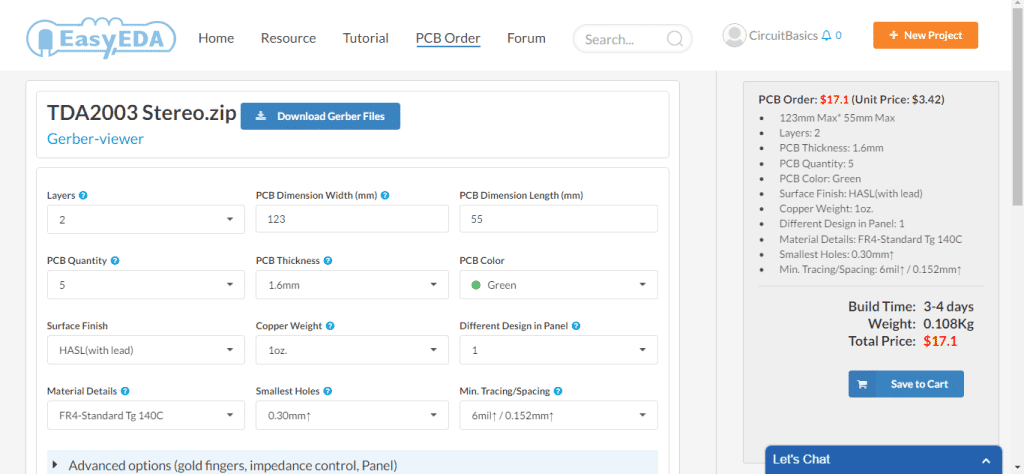
I ordered 5 PCBs for $17.10 USD and they arrived in about 10 days. The quality is great. All of the traces are routed precisely and the printing is very clear. Here’s the PCB after manufacturing:
PCB Design Tips
The power supply decoupling capacitors are placed right up against the TDA2003’s supply voltage pin (pin 5). This is to reduce the length of the traces connecting the capacitors to the chip. Longer traces have more parasitic inductance, which inhibits the flow of current.
Parasitic inductance can also cause the amplifier to oscillate when a capacitor is connected with a long trace. Oscillation will create noise in the amp’s output and may cause it to overheat. You can avoid this by keeping components close to the chip and using short traces.
The TDA2003 can be a bit tricky when it comes to grounding. Poorly designed grounding layouts are a common source of noise and hum. To keep hum to a minimum, the high current power supply and output grounds should be kept separate from the input and feedback loop grounds. This can be accomplished using a star ground. I used a star ground with a ground plane on the bottom layer of the PCB. In a star ground, each ground connection has a separate path to a central ground point. In this PCB, the terminal where negative DC power is connected to the PCB serves as the central ground point.
The ground planes help to reduce noise because they shield the circuit from radio frequencies. They also reduce the loop area of the circuit, which prevents the traces from transmitting and receiving electromagnetic fields.
For more tips on PCB design, check out our article How to Make a Custom PCB.
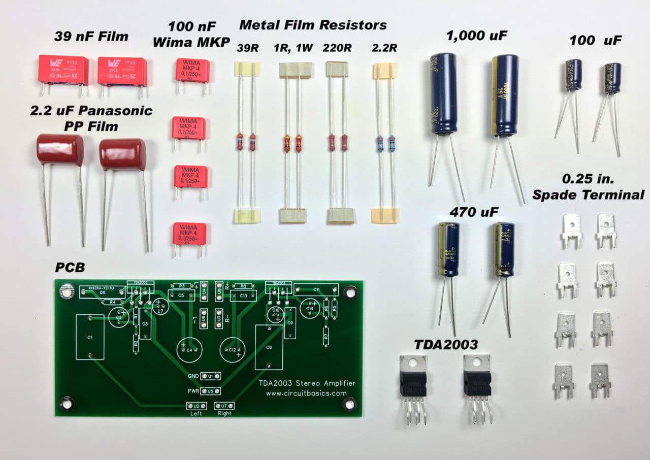
Here are the stereo TDA2003 amplifier components and PCB before soldering:
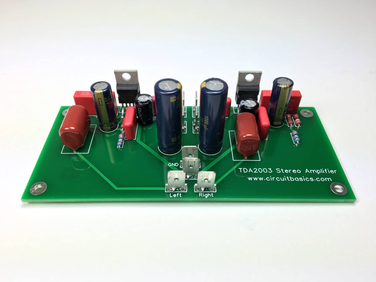
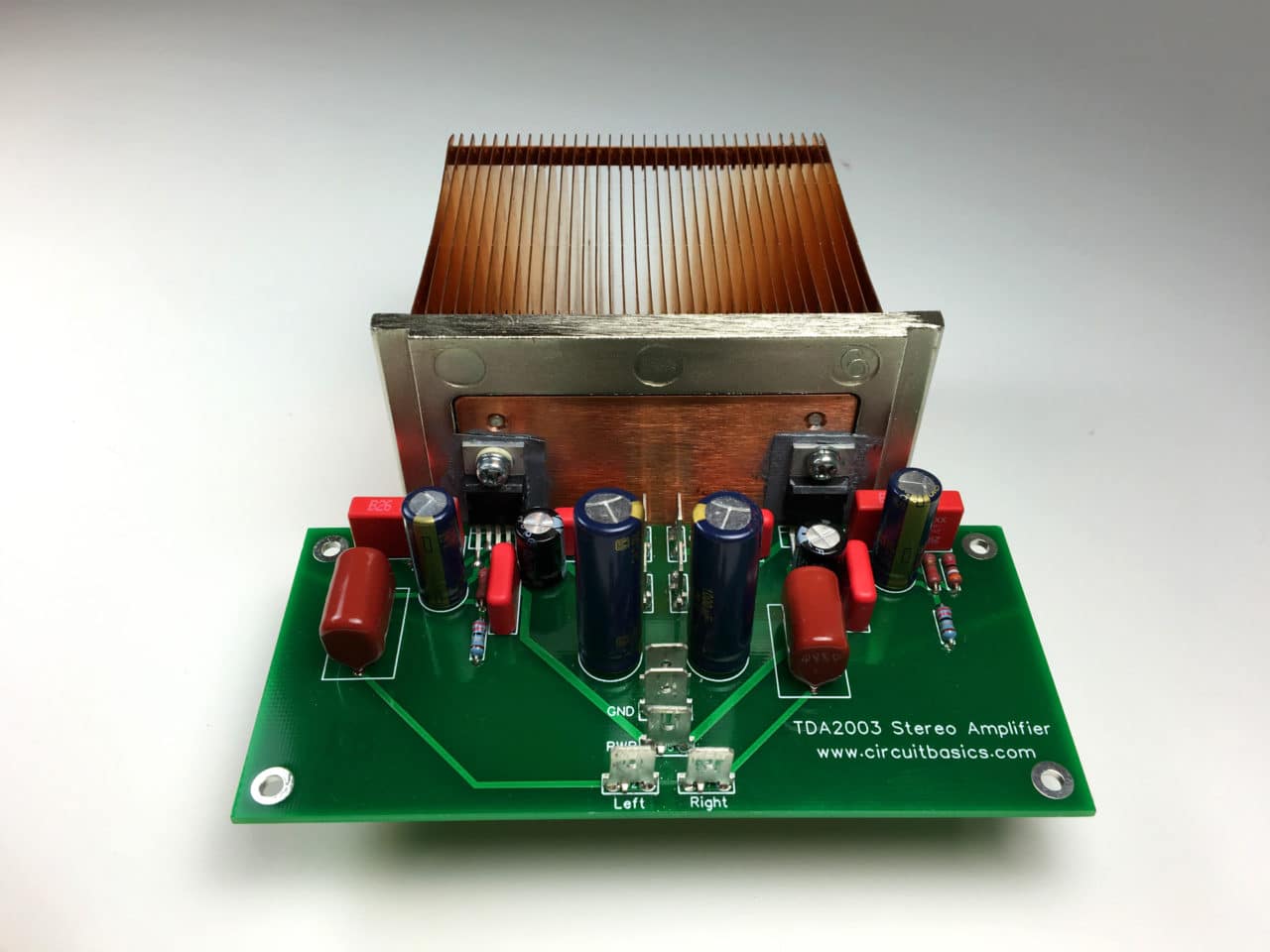
Here’s the amplifier after soldering the components:
TDA2003 Bridged Amplifier
In a bridged configuration, two amplifier chips power a single speaker. The output of one chip drives the positive speaker wire and the other chip drives the negative speaker wire. The output of one chip is 180° out of phase with the other chip, so when the output voltage of one chip is positive, the output voltage of the other chip is negative. This has the effect of doubling the output voltage, and doubling the output power into a speaker of twice the impedance. For example, in the stereo amplifier above we got 7 Watts per channel with a 12 V power supply and 2 Ω speakers. In bridged mode, we would get 14 Watts into a 4 Ω speaker with the same power supply.
Watch the video for a brief explanation of the build, and hear what the finished amp sounds like:
The Bridged Amplifier Schematic
Setting the Gain
Resistors R2 and R5 set the gain of the amplifier. Using the same formula we used to calculate the stereo amplifier’s gain, the gain of this amp is:
You can increase or decrease the gain by changing the value of R2, but I’ve found that 13.5 Vo/Vi is a good gain setting for listening in a bedroom.
Setting the Bandwidth
Like the stereo amplifier, the bridged amplifier has a low pass RC filter at the output. R6 and C6 form the filter. The cutoff frequency is calculated the same way:

With R6 at 10 Ω and C6 at 100 nF, the cutoff frequency of this filter is:

So all frequencies below 159 kHz will be passed on to the speaker.
The PCB Layout
Here is a bridged amplifier PCB layout for a single channel. For a bridged stereo amplifier, you just need to build a separate PCB for each channel:
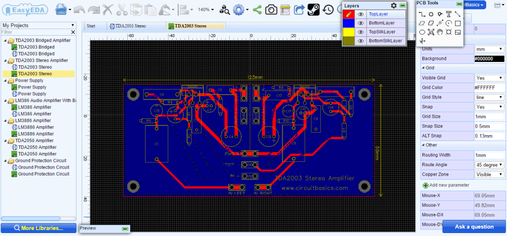
The component labels on the PCB correspond to the labels in the schematic above.
You click on the image above to edit the layout, change the component footprints, and order PCBs.
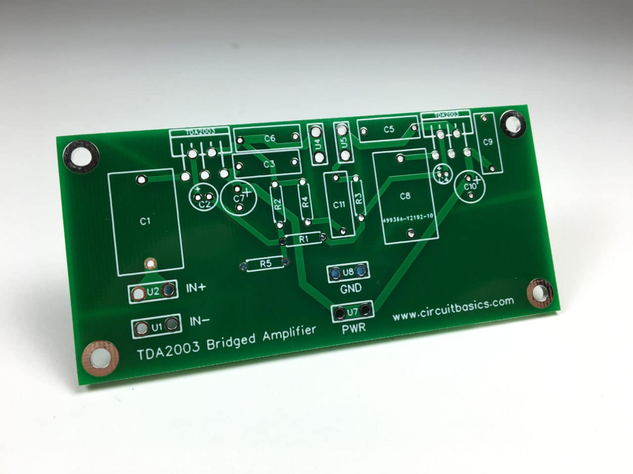
Here’s the PCB I ordered for the bridged amplifier:
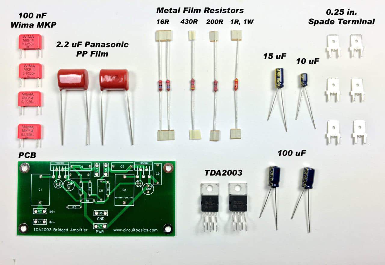
These are the amplifier components and PCB before soldering:
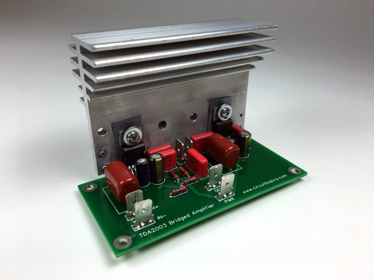
Here’s the amplifier after assembly:

Component Selection
The components you use in your amplifier will have a major effect on the sound quality. The information below should help you get the best sound without breaking the bank.
Resistors
Metal film resistors are the best choice for audio. They’re less noisy than standard carbon resistors, and are available in tighter tolerances. Better resistors will have lower tolerance and lower temperature coefficients. More expensive audio grade resistors like the Vishay-Dale PTF or Welwyn RC series are great, but you probably won’t notice much difference with cheaper metal films from TE Connectivity or KOA Speer.
Capacitors
Capacitors can be very expensive if you go for the high-end audiophile brands. However, you can still get great sound from less expensive ones. For small value capacitors less than 1 nF, polystyrene is your best bet. For values between 1 nF and 4 µF, polypropylene film capacitors are best. Wima MKP polypropylene capacitors are good (and cheap) for the 100 nF decoupling capacitors. For the larger value capacitors, electrolytics are the only option. The Panasonic FC series is great value for the money, but a step up from those are the pricier Nichicon KZ series or Elna Silmic II capacitors.
Power Supply
The TDA2003 needs at least 8 V DC and can handle up to 18 V DC with a single supply. Higher voltages will give you more output power. Figure 3 in the datasheet shows the output power vs. supply voltage curves for a given speaker impedance:
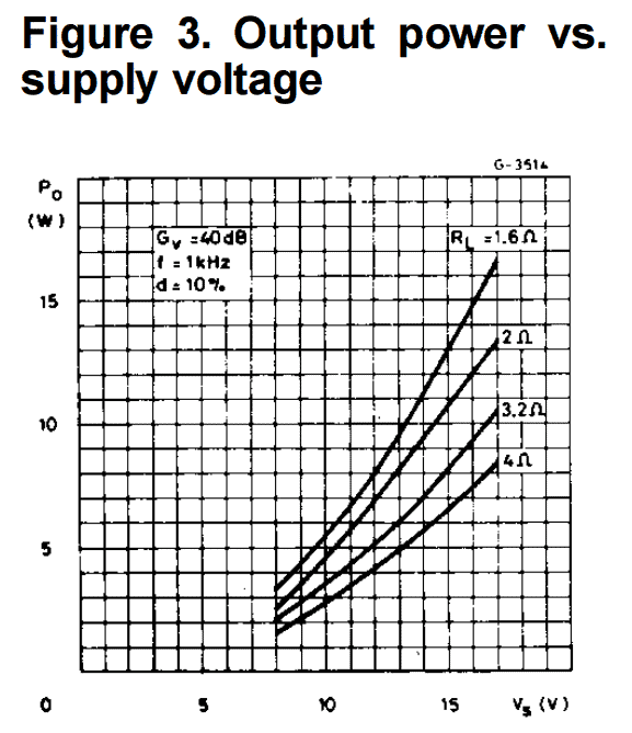
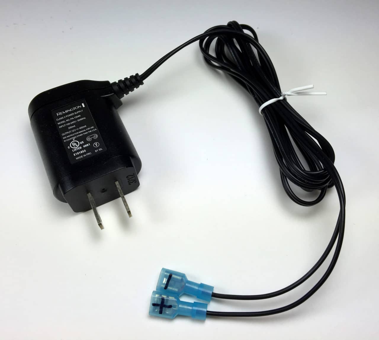
I used a 12 V, 400 mA wall plug that I scrapped from an old electric shaver and it works fine:
With this power supply, the TDA2003 stereo amplifier will output about 7 Watts into 2 Ω speakers, and the bridged amp will output about 14 Watts into 4 Ω speakers.
Heat Sinking
Each TDA2003 chip needs to be attached to a heat sink to dissipate the heat it generates. Without a heat sink the chip will get extremely hot very quickly and become permanently damaged. An aluminum heat sink sized 120 x 69 x 27 mm should work fine for two chips.
The metal tab on the back of the TDA2003 is connected to the ground pin (pin 3). If you connect two chips to the same heat sink, it’s best to isolate them electrically with an insulating washer and pad to prevent hum. For the best heat dissipation, use thermal paste on the back of the chip, the insulating pad, and the heat sink.
For the stereo amplifier, I used a CPU heat sink salvaged from an old Dell desktop I found at a thrift shop:
This is the bridged amplifier attached to another heat sink salvaged from the same computer:
Pro Tip: Old desktop computers have lots of useful components you can use in an amplifier build that will save you money. A single desktop may have as many as four heat sinks, insulating washers, a couple fans, an IEC connector and power cord, and lots of fasteners.
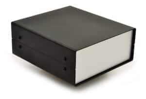
The Chassis
Installing your finished amplifier in an enclosure or chassis is a good way to make it more user friendly, and it will look much nicer too. You can use any type of box depending on what you can find, but metal enclosures are preferred since they offer shielding from interference caused by fluorescent lights, radios, and cell phones.
My favorite source for enclosures is Hi-Fi 2000. They have some very affordable and good looking enclosures that will fit the stereo and bridged amp, like their 180 x 150 mm Economy Model:
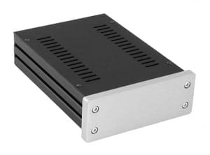
For a bit more presentable enclosure, their 124 x 170 Galaxy chassis would also fit either amplifier:
How Do They Sound?
Both amplifiers sound great. The mid frequencies are very detailed, and the highs are not harsh at all. The bass lacks a little punch, but the overall sound is very well balanced. The stereo amplifier sounds a little bit cleaner than the bridged amplifier, but the bridged amp has noticeably more power. However both amplifiers have more than enough power for listening in a bedroom. This is a great project to build if you’ve never built an amplifier before.
If you want something with a bit more power than these amps, check out our tutorial, How to Design and Build an Amplifier With the TDA2050 where we build at 25 Watt TDA2050 stereo amplifier.
If you’re looking for audiophile quality sound, we also have a build guide for a 40 Watt Hi-Fi LM3886 Amplifier. These amps are a bit more complicated than the TDA2003, so if this is your first chip amp project I’d definitely suggest starting with the TDA2003.
Well, thanks for reading and hope you got something out of this article. If you have any questions, be sure to let us know in the comments…


Hello,
I see your project very interesting.
I like this.
I have the questions for this project:
1. I added 2 variable resistors 10k before the capacitors C1 and C2 to adjust volume for the left channel and the right channel. Is that right?
2. If I right, How to use only one variable resistor for adjusting the volume on 2 channels?
Thanks,
Sy Do
Hi Sy Do,
Yes, you’re right, to adjust the volume you need to put a variable resistor before C1. If your’re building a stereo amp though, you want the volumes to be adjusted equally on both channels without having two separate potentiometers. For that you can use a “dual gang potentiometer” which is basically two potentiometers controlled by the same knob. Here’s an example of one:
https://www.amazon.com/gp/product/B0173E0CYY/ref=as_li_qf_sp_asin_il_tl?ie=UTF8&tag=circbasi-20&camp=1789&creative=9325&linkCode=as2&creativeASIN=B0173E0CYY&linkId=b3a031661b0d5fe4c55bd0593c59b4ec
Does any circuit do this instead of using “dual gang potentiometer”?
Hi, Thank you for your useful information
can I use the LM380 instead of TDA2003 in the above circuit?
AWESOME! Post. It gives me a clear conception about BRIDGED AND STEREO AMPLIFIERS.
Thanks for sharing.
I have a question about the bridged Amp: where do I need to place my potentiometer, in order to be able to adjust the volume? and what value does it need to have if my input source has a maximum voltage of 2Vrms?
Hi,
Electronic circuits is a total new hoby for me and I found this site and it is a good start.for me.
I am for several weeks ordering the parts from the partlist and they are finally at home.
Now I did the final check befor starting solder the bridged amplifier.
I do not mean it critacal but I see some differences in the pictures from the amplifier relative to the PCB before soldering.
There is part missing namely: C5 47 nF Xicon Polystyrene and I am wondering when it is added? And when you order it by Mouser from the partlist it is an 4.7nF a diffent value. For me (I am not an electrician) it is very confusing. Mabey you can say something about this point before I solder. I wonder if it is possible to replace this capitator for a (M) KP capitator with the same value?
my dear Frit,
Value of capacitor C 5 is 47nF that is equal to 47kpf or 0.047 mfd You can use any one
How much maximum output can tda2003 give in reality if built using the components given in test circuit ?
I have heard that no amplifier can give it’s full output as mentioned in datasheets so I wanted to know
I wanted to ask, what is the resole that you used, high voltage capacitors in a circuit that will work on a supply of 12 Volts.
12dc is the voltage required for activating chip circuits but into different paths of the circuits AC current is passing and that ac current with its high frequency generates high voltage at different stages hence high voltages capacitors are used there.
Hi, could I use this amp suitable for headphones? Would I have to modify/add something to the circuit? Thanks!
Hi !
I am wondering if you have posted a circuit with the (venerable, obsolete but still available) TDA2030A, especially in BTL mode.
I would be obliged if you did that.
OR
Alternatively can I safely assume that the TDA2030A can be substituted in the TDA2050 bridge circuit but with a different power supply and thus different components values? If yes, what would these PSU requirements and new component values would be.
Thank you!
I’m planning to build and test a bridged version with a 18V supply. Does this have any impact on the ratings of any componants. Also is there any form of tone control that could be used?
How can you get 7W or 14W from a power supply of only P=12V*0.4A => P=4,8W.
That’s the reason of poor bass.
Not enough power from the power supply.
You need at least 12V / 1.3A = 15W for the 7W audio version,
and at least 12V / 2.5A = 30W to the 14W audio version.
These values must be doubled for a stereo version.
Keep in mind that this IC TDA2003 is intended for car audio,
and the car battery can deliver a lot more current then 0.4A,
so it sounds also a lot better.
This is assuming that efficiency is around 50 to 60%.
Nevertheless the old TDA2003 AB class is a bit better then that.
Hi , the datasheets show the frequency upper cutoff being dependant on the relationship between Cx and R1 , not Cx and Rx. Hence C6 and R1 or C11 and R6.
Also , in the bridged amp the 15u cap is the other way round in the datasheet.
Sorry , I meant the 10uf cap is the wrong way.
Hey, I just built this amp – sounds great but I get some hum when there’s no input signal. I’m just testing it, with the circuit board and heat sink sitting on a table, like in your video. You were getting hum when you touched the input jack. I am getting some hum even when not touching the jack & when the jack is plugged into my laptop which I’m using as a music source to test.
If you could give me any ideas what to check on to solve this issue, I’d greatly appreciate it! FYI I did order and use the PCB from this web page.
Thanks!
Hello, thanks for your interesting and inspiring projects. I have a doubt on the ‘SETTING THE BANDWIDTH’ chapter: in my knowledge the range of human hearing is between 50 Hz and 20000 Hz. The TDA2003 datasheet is stating that the frequency response of the IC is between 40Hz and 15000Hz: how comes the ‘frequencies below 104 kHz are output to the speakers’?
In the same datasheet the setup of frequency response is reported as linked to the gain settings and calculated based on the formula 1/(2PI*B*R1) where B is the upper cutoff frequency and R1 is the gain settings resistor. I am quite confused on that part, can you help me to understand?
Thanks in advance!
Hi
I want to use a raspberry pi as audio source and connect this amp to ceiling speakers. It will only be used as soft background music. Will this setup work? I assume i will be able to set the volume up/down on the raspberry pi?