
To understand why electronic evolution has led to a much more complicated way of making regulated power supply units, we need to go back a bit and look at linear power supplies.

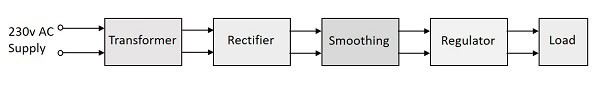
Linear power supplies are simple, reliable, and quiet PSUs with good regulation and low ripple—so why change? There are two main reasons, and both relate to cost. First, linear power supplies require large and expensive transformers. Second, the regulating transistor generates a lot of heat, which requires large and expensive heat sinks. For example, a 50V variable power supply set to output 5V at 2A might have (50V – 5V) * 2A = 90W of heat to dissipate.
A switched mode power supply (SMPS) nearly eliminates both of these issues, but the circuit becomes more complex.
How a Switched Mode Power Supply Works
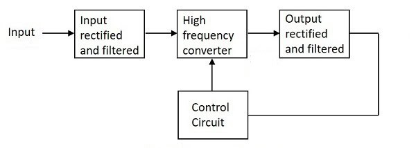
In the block diagram above, the mains are fed directly into the first block without using a transformer. Of course, diodes and capacitors used here must be up to the job. Note that DC could also be fed here, for example, in a 12V to 5V DC to DC converter. The incoming AC mains current is now a high voltage rectified DC current.
The next block is the high-frequency converter, a chopper circuit turning a power device such as a MOSFET on and off at several kHz. This is a high frequency transformer that converts the incoming DC to a square wave.
The next stage once again rectifies this and filters out ripple and noise. The last block, the control circuit, is where the magic happens. This is a feedback circuit controlling the chopper MOSFET.
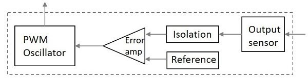
The control circuit has a voltage divider/multiplier that senses the output voltage. Because we will feed this back to the chopper circuit running at hundreds of volts, it needs to be isolated, usually with an optocoupler. There is a reference signal generated by a fixed reference diode or trimpot. The error amp compares these two voltages and adjusts the PWM (pulse width modulation) oscillator, which controls the MOSFET.
Putting it all together
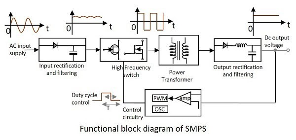
The functional block diagram above gives a better and more detailed look at the parts involved.
Practical Example
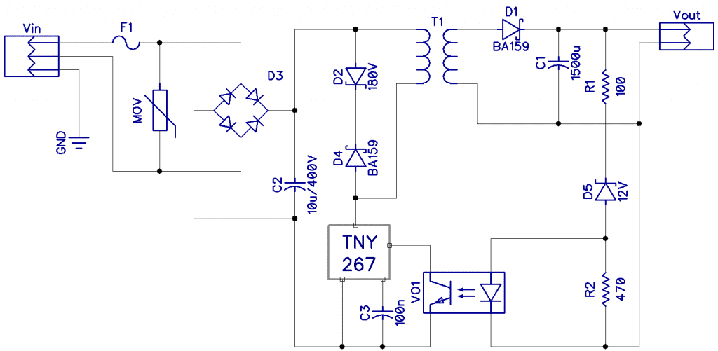
Shown below is a straightforward yet working switch mode power supply. The heart of this circuit is the TNY267 switching regulator. This one IC performs the functions of the PWM generator, MOSFET chopper switch, error amp, and control circuit.
The final output of this circuit is 12V, and it can deliver 1A:
Notes on the Circuit
- Vin is a 100-300V AC mains connector.
- MOV is a metal oxide varistor, used to protect the circuit from high voltage spikes.
- D3 is a full-wave bridge rectifier, and the DC output appears across capacitor C2. With a 220V AC input, this would be about 220V * 1.4 = 308V DC, so be careful!
- D2 is a 180V transient suppression diode to handle back EMF spikes.
- The TNY267 runs at about 132kHz.
- Diode D1 (Schottky) on the secondary rectifies the 132kHz AC, and capacitor C1 smooths out the ripple.
- Capacitor C3 is a required bypass capacitor.
- Resistors R1, R2, and diode D5 provide a feedback circuit to the TNY267 via an optoisolator to ensure there is electrical isolation from the mains at all points.
- The primary of transistor T1 is 157t, and the secondary is 14t. The core is an E19 type ferrite transformer with a central core of about 4.5×4.5mm.
Parts of the circuit above contain very high AC and DC voltages. Make absolutely certain that the components you use are rated to handle such voltages. And never work on high voltage devices unless you are fully trained and competent to do so.
Now, we know how much more efficient an switch mode power supply can be, yet it is more complex and requires quality components for reliability.
Thanks for reading and be sure to leave a comment below if you have questions about anything!
Images used with permission from www.tutorialspoint.com.


Thanks very useful. However, I couldn’t see any comment on D4. Is this the same as D2?
Hi,
According to the text, the MOV is rated 275V and the input AC voltage is up to 300V. How come the MOV could work normally when the input voltage is at the high limit? (peak voltage = 300V * 1.4 = 340V).
Hi, There is a typo error. T1 is a transformer, not a transistor.
Bonjour et merci pour ce tutoriel , j’aimerais savoir comment est-ce que vous avez dimensionné le transformateur car moi je travail sur un cas particulier ou je dois fournir en sortie une tension de 3V / 250 mA
What gauge magnet wire would you recommend for the transformer primary and secondary? It seems to me that it would have to be 20GA or larger to carry 1amp of current. If so, it would seem nearly impossible to get 157 turns on an E19 coil form
Think equivalent power – for a pri:sec ration of 157:14 (about 11:1) you’ll expect the primary to be rated around 1A x 11 / 157, around 100mA – so you can use a lower gauge wire.