An amplifier is a circuit that takes an electronic signal at its input and produces a larger signal at its output. This generally refers to voltage, but it could also be current, noise, or power. In this article, we will look at the most common and useful voltage amplifiers. These are generally classified as audio amplifier (AF) or radio (RF) amplifiers. The range of frequencies defines them, and this, in turn, determines the type of components to be used.

Audio amplifiers are amplifiers that work between 10Hz and 30kHz. Radio amplifiers work above that right up to several GHz.
For the sample project, we will use an audio amplifier in the 0-20kHz range, with emphasis on low noise and low distortion. We will also use a radio amplifier, typically from 500kHz to tens of GHz, with a gray area in between usually for ultrasonic and video, which could use both techniques. Radio signal or RF amplifiers are a completely different kind of amplifier and will be covered in detail in a separate article.
Gain
Gain refers to the amount of amplification and the ratio between the output and input signals. Voltage gain would normally refer to small-signal amplifiers (e.g., op-amps); power gain would be used for power amplifiers (e.g., Hi-Fi amplifiers or transmitter amplifiers). We may refer to gain as “times” or “X,” i.e., 10X, which means that the voltage at the output is ten times bigger than the input voltage. It is worth mentioning that they may have different resistances affecting the useful power that can be supplied. Gain is also often specified in dB where,
![]()
and power gain as
![]()
This means that a voltage gain of 10 times is 20log10 or 20dB, and a voltage gain of 100x is 40dB.
But why do this? Each one might have different gains in a system with multiple stages, and in RF systems, even attenuation. Hence, you just add them up to get the total system gain.
In a power amplifier, this becomes more important. Say you have an amplifier with an input resistance of 50kΩ and an output resistance of 8Ω, and you measured the voltage on the input as 10V and the voltage on the output as 10V. You might be mistaken to think that the gain is 1. The power at the input is V2/R = 102/50k = 2mW. The power in the output is 102/8= 12.5W. This is a power gain of 10log(12.5/2* 10-3) = 38dB whereas the voltage gain is 0dB.
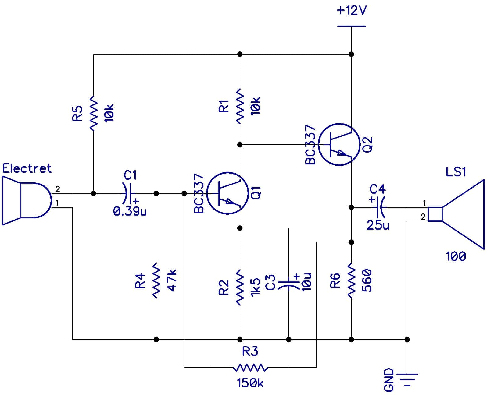
Common Emitter Amplifier with Electret Microphone
Designing a transistor amplifier is not that difficult. There are just some assumptions that you’ll need and some data about the transistor you will use. The choice of the transistor depends on the frequency range and the power level. Here, we are making a small signal AF amplifier and can use any of the hundreds of transistors. So let’s use the well-known BC337.
How the circuit works
Our design begins with a look inside the transistor itself.
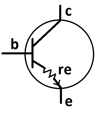
In the emitter, there is a ‘hidden’ resistor Re. You can’t measure it with a multimeter, but it’s there. Re has a dynamic value dependent on the collector current Ic such that Re = 25/Ic, where Ic is in mA. So if Ic is 10mA, then Re = 2.5Ω. The other important thing to know is that the transistor’s current gain can be approximated as Ic/Ib and is called hfe. Typically, 50 to 1000 for small transistors. The transistor choice in this design is not an issue; almost any small signal NPN type will be fine.
For any transistor to work, it needs to be biased. This means that the base is raised or biased 0.6V higher than the emitter. Besides that, we also need to think about signal headroom and input impedance. Any voltage that we set up on the input is going to affect the voltage at the output. The voltage at the output is a DC offset, and we want to make this work in our favor. The choice of the collector resistor and the current through it will govern this.
The first assumption is what this circuit will be driving—what output resistance must it have. We should have an output resistance at least 2x to 5x lower than the next stage. So let’s assume the next stage input resistance will be 47k and make our output resistance 10k. We do this simply by making R110k (this is a bit of a simplification but is close enough).
The next assumption is that we don’t want a distorted output where one of the half-cycles clips. We want to set the collector voltage of Q1 to be half-way. So if R1 is 10k and the voltage across it is 12/2, i.e., 6V, the current through R1 is V/R = 6/10000 = 0.6mA. This is our collector current, and we can now find re=25/Ic = 42Ω. We will use this later.
For stability and good biasing, we would like the emitter of Q1 to be at about 1V. This will allow a reasonable signal swing at the base of Q1. So to get 1V across R2 knowing the current through it is 0.6mA, R2 = V/I = 1/0.6 = 1.6k, let’s make it 1k5. This will change the voltage on the emitter slightly so V=IR = 0.6* 1500 = 0.9V.
Now, the voltage on the base will ALWAYS be 0.6 higher than the emitter, and the current into the emitter will be Icollector/hfe. The datasheet for the BC337 shows an hfe of 600. Let’s assume a bit less to be safe, say 200. So Ibase is 0.6/200 =0.003mA. For stability, we will make the current flowing down the divider chain R3, R4 ten times bigger, i.e., 0.03mA, so the voltage across R4 is 0.9 + 0.6 = 1.5 and the current through is 0.03, R4 = V/I = 1.5/0.03 = 50k. We make it a standard value of 47k. This slightly changes the current to 1.5/47k = 0.032mA. R3 has 12V on one end and 1.5 on the other. The voltage across it becomes 12-1.5 = 10.5V, and so R3 = V/I = 10.5/0.032 = 328k. Make it a standard value of 330k. R5 has nothing to do with the transistor design. It provides a voltage to supply the electret mic (it has an electrostatic capacitor coupled to a small FET inside), and 10k is a usual value.
Now, how much gain can we expect? The gain will be R1/R2+re = 10k/ 1k5+42 =6.48. This is not that useful, but we can increase this by AC bypassing R2 with a capacitor C3 leaving only re. The DC conditions remain the same, but the gain is now 1500/42 = 35. We must make C3 with a value such that its reactance is equal to R2 at our lowest frequency, 40Hz, so C3 = 1/2πfXc = 2.6uF. Hence, make it 10uF.
The remaining design is for the input and output capacitors. C1 is easy. The input resistance is a combination of R3 in parallel with R4 in parallel with R2+re*hfe, (1k5+42)*200 = 300k. It is pretty much just a bit less than R4, say 40k, but it needs to have a capacitive reactance equal to R4 at the lowest frequency we intend to amplify. If we choose 40Hz Xc = 1/(2πfC), then C = 1/2πfXc = 0.39uF. In the same way, C2 = 1/2π40*10k = 0.4uF. Hence, make it 1uF.
The next step in our design is to add a buffer transistor to increase the output drive capacity to enable a small (high impedance) speaker. This is called an emitter follower. It has no voltage gain, but it has a much lower output impedance. We will also provide some DC negative feedback to ‘lock’ the bias of Q1.
The only components that are going to change are R3 and C4; C2 has been replaced with C4. Without C4, there would be a DC offset across the speaker. We need to know what the impedance of the load is, i.e., the speaker. This simple circuit cannot drive an 8Ω speaker; you would need a power amplifier for that. Assuming we are using a cell phone earbud at about 100Ω. For a 12V pp swing that would be about 1W, which is pushing it for this simple circuit, the emitter follower’s static DC power should be equal to that to result in 100mA in the transistor, which is way beyond its means. We are going to back off our expectations and allow a maximum of 10mA in Q2. As Q2 emitter is 6-0.6V = 5.4V then R6=5.4/0.01 = 540, call it 560Ω. R3 is now no longer connected to 12V, but to 6V, its value becomes (6-1.5)/0.03 = 150K. C4 is now 1/2π40*100 = 25uF.
Final Values
Verified Results
The design was assembled on a breadboard to see how the results matched our design.
DC conditions (no signal):
Q1 collector 6.8V, base 1.36V, emitter 0.98V, all pretty close!
Q2 emitter 6.1V, perfect!
AC results with signal generator input and no load on output:
Without C3, Vswing with no distortion 9.6Vpp for 1.68Vpp input, gain of 5.7.
Estimated gain was R1/R2 = 10/1.5 = 6.6.
With C3, Vswing with no distortion 6.7Vpp for a 50mV input ie gain of 6.8/0.05 = 136.
Estimated gain 10k/42 = 238 an unexpected difference? This is due to the series resistance of C3 not being zero.
This little amplifier is not really suitable to drive a speaker of average impedance. I connected a 300Ω headphone and found by substantially increasing the collector current in Q2 by making R6=390Ω. I was able to get an undistorted output swing of 4Vpp.
So we have done a rigorous component level design of a two-stage audio amplifier. If you follow these design rules, you should be able to design one of your own.

In the paragraph where the gain is calculated the result is 35 with the use of C3. It’s a wrong result wich is corrected in a later paragraph.
Also, I don’t understand how you did found that an earbud of 100 Ohms over a peak-to-peak voltage of 12V would consum a power of 1W.
Beside that, I found the article very useful and very clearly explained.
Many thanks.
Lahcene