In this article, we will look at the internal physics of transistors.

In a famous diagram showing how a transistor works (Figure 1), the “transistor man” watches a gauge measuring the base current (IB) coming into the transistor. He then multiplies the base current by the transistor’s hFE and turns a potentiometer to set the collector current (IC) to match the value defined by IC = hFE * IB .
How Transistors Work
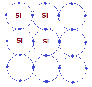
Silicon is a semiconducting material that has four electrons in it’s outer electron shell. The semiconducting properties of silicon can be improved by adding impurities such as phosphorus or boron in a process called doping.
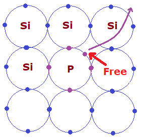
Figure 2 below shows pure silicon neatly bonded in a crystalline lattice. The dots are electrons. Figure 3 shows the lattice when silicon has been doped with phosphorus.
The phosphorus atom has five electrons, so one electron is displaced. This electron is free to move about in the material. This is how N-type semiconducting materials are made. Applying a voltage across the material encourages electron flow.
 |  |  |
| Figure 2 | Figure 3 | Figure 4 |
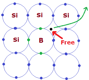
Figure 4 shows doping with boron which has one less electron. The absence of the electron creates an electron hole. Electron holes can move freely around the lattice. This is how P-type semiconducting materials are made.
In transistors, these N and P type semiconducting materials are bonded together to allow the ability to control the direction and flow of electrical current.
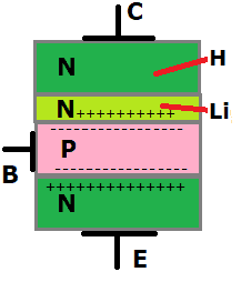
The bipolar NPN transistor shown below uses both electrons and electron holes as charge carriers:
The lower P and N junctions are sandwiched together. The upper N-type section has a heavily doped region and a lightly doped region. The heavily doped section is connected to the collector terminal, the P section is connected to the base, and the lower N section is connected to the emitter.
When the N and P type layers are sandwiched together like this, all of the free electrons in the N-type material cross the junction and gather at the bottom of the P-type material, filling the electron holes:
Electron holes also form in the bottom N layer, forming what’s known as a depletion region. Likewise, a depletion region also appears in the upper N-type layer, effectively making it high resistance.
As shown in the diagram below, since we have a small current in the base and a large current in the collector, we effectively have current gain. This is how a BJT or Bipolar Junction Transistor works. The NPN and PNP versions are precisely the same, except that all of the layers and applied voltages are reversed:
Suppose a slowly increasing positive voltage is applied to the base. In this case, no current flows, but the depletion region becomes thinner and thinner until at about 0.6V the barrier is overcome and it starts conducting current. This allows electrons to flow from the emitter to the base:
Applying a positive voltage to the collector will also attract electrons from the lower N region and start a current flow (blue arrow). The highly doped region forms a lower ‘resistance’ than the lightly doped region. This creates a potential difference, which concentrates charge near the junction. The higher positive charge in the lightly doped region attracts all the free electrons in the lower N region, which rush towards the collector.
FETs and MOSFETs
Shown below is a typical JFET or Junction Field Effect Transistor. Although the construction is very different from the bipolar transistor, what goes on is very similar.
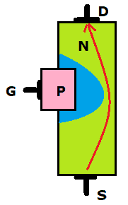
The P and N junction forms a depletion area as before, so no charge carriers are available to conduct. Hence, the drain (D) and source (S) have a high resistance between them. Field effect transistors break down the depletion layer by applying a positive voltage to the gate (G), allowing the current to flow between the drain and source (red arrow in the diagram above).
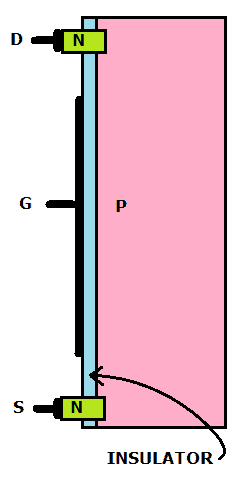
Metal Oxide Field Effect Transistors, or MOSFETs, have a thin metal oxide insulating layer separating the gate from the P-type material. Applying a positive voltage to the gate creates a field in the P-type material, which again clears the depletion region creating a conduction channel. This allows current to flow between the drain and source.
FET Symbols
Below are the different schematic symbols for N-channel and P-channel JFETs (left) and MOSFETs (right):
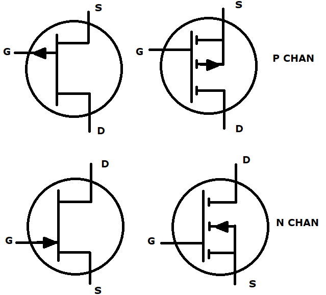
Note the direction of the arrows. They indicate if the transistor is a P-type or an N-type. Also, note the gate symbolically shown as separate from the drain-source channel in the MOSFET transistor.
Hope this article has helped you understand how transistors work! Leave a comment below if you have questions about anything.


I found it interesting that we picked nearly the same topic for our blogs this week. I wrote about Julius Edgar Lilenfeld, inventor of the modern transistor. I linked my readers to your excellent post on how the transistor works, It thought your readers might enjoy reading the history at https://www.techshepherd.org/history/unsung-hero/