
Breadboards are great for prototyping circuits, but they aren’t so good for actually using the thing you’re building. At some point you’ll probably want a more permanent solution, and the best way to do that is to put the project on a PCB.
In this tutorial, we will walk through the process of converting a schematic to a PCB layout and getting it produced by a custom PCB manufacturer. The performance of a circuit depends greatly on how it’s laid out on a PCB, so we also provide information on how to optimize your PCB design.
Using the right PCB design software is important, so be sure to check out our article on the The Top Five EDA/eCAD Programs for Circuit Design to find the best program for your needs.
Start With a Schematic
Before you start designing a PCB, it’s essential to have a schematic of the circuit. The schematic will serve as a blueprint for laying out the traces and components on the PCB. Most PCB design programs will import the component footprints and wires from the schematic into the PCB file, which makes the design process much easier and faster.
Component Footprints
Each symbol in the schematic needs to have a PCB footprint associated with it. The PCB footprint will define the component’s physical dimensions and placement of the copper pads or through holes on the PCB. This is a component footprint for the LM3886 audio amplifier IC:
The footprint defines the component’s length, width, number of pins, pin layout, diameter of through holes, and more depending on the particular component. Now is a good time to decide which components you’ll be using.
Footprints for common components are included with most EDA/ECADS. But you might need to create your own footprint for some unusual components. Most EDA/ECADs have modules that can do this easily using dimensions from the device’s datasheet.
You can also find the footprint’s for many components online, so check there first before creating your own.
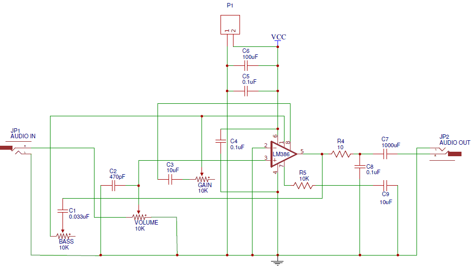
Once you’ve assigned component footprints to each schematic symbol, it’s time to start drawing the wires. Rather than explain the details of that here, I’ve made a video so you can watch me draw a schematic for an LM386 audio amplifier in EasyEDA as an example:
Organize the Circuit Into Sub-Circuits
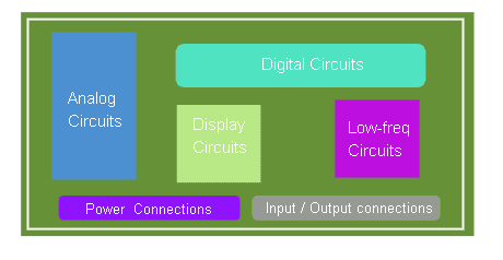
The first thing to do is identify what each part of your circuit does, and divide it up into sub-circuits according to function. Keep the components in each sub-circuit grouped together on the PCB. This keeps the track length between components short. Here’s an example of different sub-circuits grouped together on a PCB:
Arrange components like resistors, capacitors, and transistors in a way that minimizes the length of the conducting traces. Long traces can pick up electromagnetic radiation from other sources which can cause interference and noise.
Aligning similar components in the same direction is also a good practice. This will give the PCB a more efficient and logical design.
Sub-circuits that dissipate heat or generate electromagnetic fields (EMF) should be positioned away from sensitive components. For example, in an audio amplifier the noisy power supply is always placed far away from the sensitive audio input circuit.
Daisy Chain vs Star Topologies
When deciding how to connect the different sub-circuits on your PCB, there are two common methodologies to consider – the daisy chain topology and the star topology:
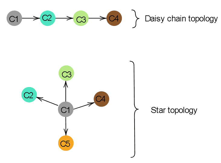
These topologies are used to describe how sub-circuits (C2-C5) are connected to a power supply sub-circuit (C1).
In a star topology, multiple sub-circuits are directly connected to a central power supply. The advantage of the star topology is that if one sub-circuit fails, other sub-circuits will remain functional. It also ensures that each sub-circuit gets an equal supply voltage.
A daisy chain topology is when one sub-circuit is connected to another in a chain. A daisy chain topology reduces the length of traces and saves space on the PCB. But if one component fails, components further down the chain might also fail. It can also create a voltage drop and result in lower voltages at sections further from the supply.
In general, especially in audio circuits, the star configuration is preferred since the voltage drops caused by the daisy chain topology can create noise in the return path and reduce the available current supplied to parts of the circuit.
How to Route Traces to Minimize EMF Noise/Interference
A moving charge produces a magnetic field, and a magnetic field can produce an electric field. On a PCB, electric currents are flowing in different directions and magnitudes through the conducting traces. If a PBC is poorly designed, parts of the circuit can act as an antenna that generates or picks up electromagnetic fields (EMF). EMF can generate unwanted electric currents in circuits, leading to noise or unpredictable effects in sensitive integrated circuits. Electromagnetic interference should be minimized in circuits when possible.
Here are some ways to minimize EMF interference in a PCB design:
- Keep all traces as short as possible
- Avoid creating loops with traces
- Avoid 90° angles in trace bends (use 45° angles instead)
- Keep high speed signals separate from low speed signals
- Keep return paths short
- Route single supply (Vcc) traces close to ground paths
- Route differential (+/-) traces as close to each other as possible
PCB Shape and Size
Most PCBs are designed to be square, but round, triangular, and other interesting shapes can be made as well. The shape of a PCB can be defined by setting dimensions for the PCB outline in the PCB design software.
If the PCB will be mounted inside of a box or housing, the dimensions of the PCB cannot exceed the inner dimensions of the housing. It’s important to know the dimensions of any enclosures that will be used before laying out the PCB. For a better fit and easier installation, allow a few millimeters of space between each side of the PCB and the inner wall of the housing.
The components will also have an effect on the size of the finished PCB. For instance, surface mounted components are small and have a low profile, so the PCB can be smaller. Through hole components are larger, but they’re often easier to solder.
User Interfaces
Carefully consider the location of user interfaces like buttons, switches, potentiometers, LEDs, and power inputs, as these can limit the ways a PCB can be laid out. Need an LED placed next to a power switch to indicate that the device is powered on? Or need a volume potentiometer to be placed next to a gain potentiometer?
For ease of access, it is usually a good practice to place any power supply connections or other input/output connections near the edge of the PCB.
For the best user experience you might have to make some compromises and design the rest of your PCB around these components.
Heat Management
Some components generate heat when an electric current flows through them. Potential heat sources may include voltage regulators, op-amps, transistors, and even copper traces and vias. You might need to employ heatsinking to remove excess heat from these devices.
If your PCB is already assembled, you can use a thermal imager to measure the heat signature of the PCB while it is operating. This can help you to identify components or sections that are emitting excessive heat.
If heat is an issue, consider replacing linear voltage regulators with switching voltage regulators. You can also use heat sinks or cooling fans. However, this could make the overall package larger and heavier.
Heat can also be dissipated from a component by using thicker copper traces. For dissipating heat away from SMD components, thermal via arrays are commonly used.
Single-Layer PCBs
One of the first choices to make in PCB design is the number of layers to use. There are a lot of factors that might influence this decision. For example, the complexity of your circuit, manufacturing costs, pin density, signal layers, operating frequency, and PCB turnaround time, among others.
For most hobby projects, single or double layer PCBs are the easiest to design. Shown below is a cross section through a single layer PCB:
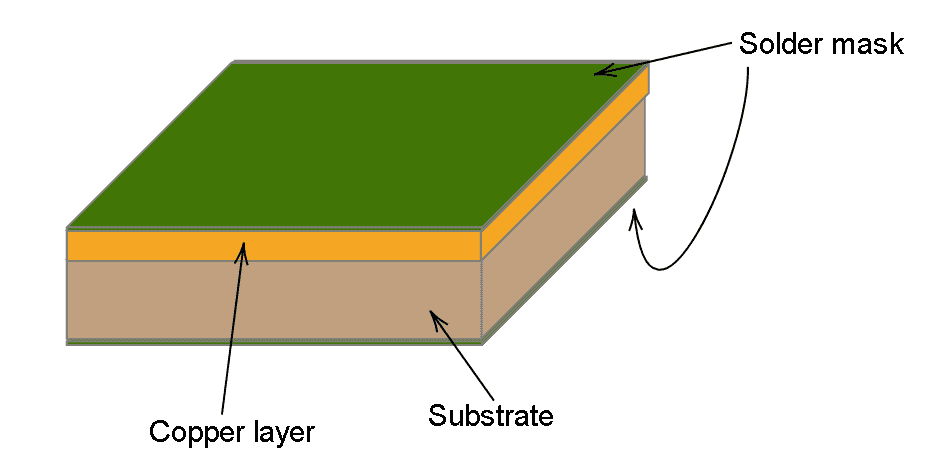
A single layer PCB has just one copper layer on the top of the PCB. This copper layer will be etched with your PCB layout files, leaving only the copper traces on the PCB. Single-layer PCBs are cost-effective, easy to understand, and convenient for manufacturing.
Double and Triple Layer PCBs
Larger circuits can be difficult to design on a single layer PCB. As design complexity increases, it gets harder to route the traces without intersecting one another. Luckily there are double, triple, and multi-layer PCBs that allow traces and planes to be routed on electrically isolated layers.
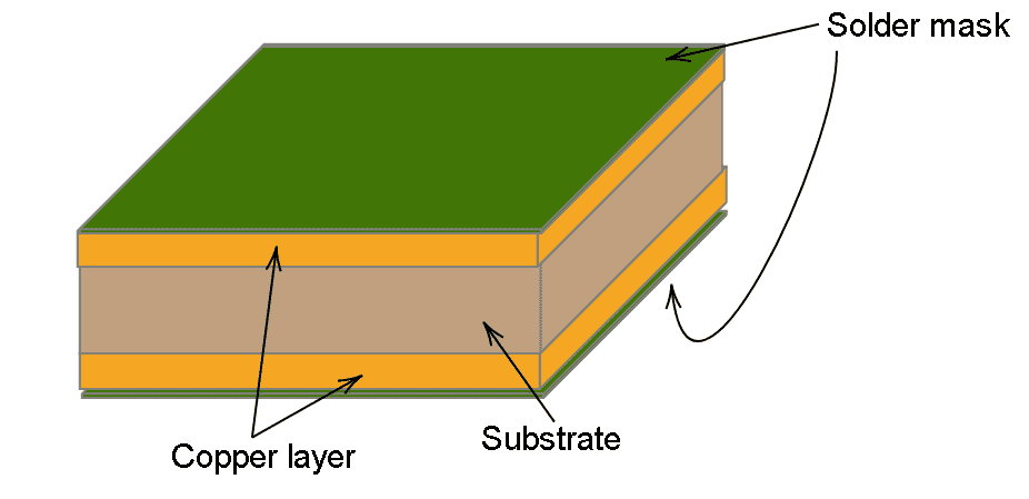
Double-layer PCBs have two copper layers, one on top and one on the bottom:
Three-layer PCBs have a copper layer sandwiched between the top and bottom layers:
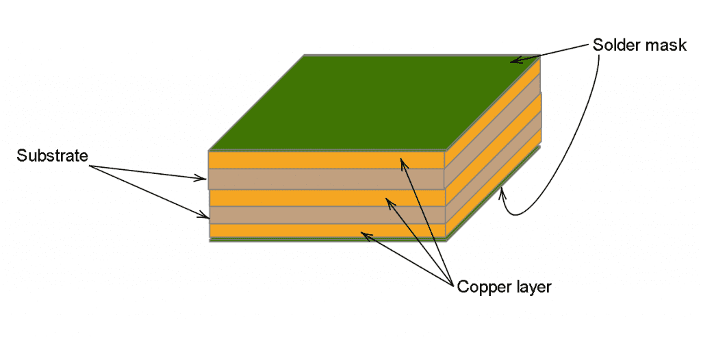
Multi-layer PCBs pack even more copper layers inside the PCB. Very complex PCBs have up to 100 layers!
Connecting the Layers
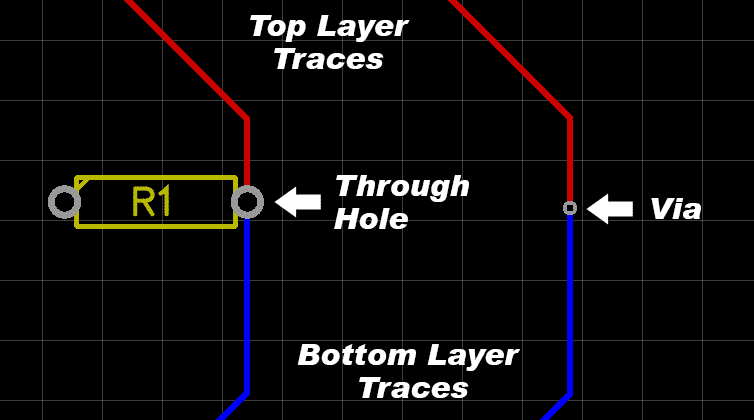
When designing a multi-layer PCB, you may need to create links between the various layers of your PCB. You can use a via or a component through hole to achieve that.
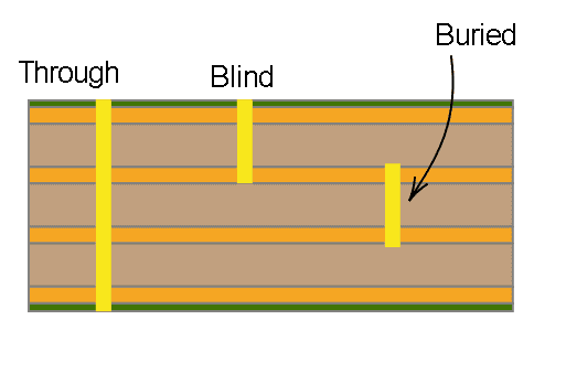
In Latin, via means a path or way. In the context of PCBs, vias create an electrical connection between layers in the PCB. Basically, a via is a conductive hole that has copper pads on each layer.
The three main types of vias are through-hole, blind, and buried:
You can also connect layers with a component’s through hole. This image shows the difference between a through hole and a via connecting top and bottom layer traces in a PCB design program:
Ground Layers and Power Planes
A ground layer is a layer of copper covering large parts or the entire bottom of a PCB that is connected to the circuit’s ground terminal:

Ground layers are a great way to supply ground to circuits for several reasons:
- Many traces can be shortened or even eliminated
- The large copper area shields against electromagnetic fields
- The copper area dissipates heat
- Reduces the loop area of traces, reducing EMF interference
Using copper planes for the Vcc, V+, or V- power supply traces is also beneficial. Routing wide power supply traces over a ground plane minimizes the loop area of the circuit and reduces EMF interference in the power supply. Power planes are usually added to the top of a single layer PCB or to the middle of a two layer PCB.
Layer Thickness
Most PCB manufacturers will let you order different layer thicknesses. Copper weight is the term manufacturers use to describe the layer thickness, and it’s measured in ounces.
The thickness of a layer will affect how much current can flow through the circuit without damaging the traces. Trace width is another factor that affects how much current can safely flow through the circuit (discussed below).
To determine safe values for width and thickness, you need to know the amperage that will flow through the trace in question. Use an online trace width calculator to determine the ideal trace thickness and width for a given amperage.
PCB Traces
If you look at a professionally designed PCB, you’ll probably notice that most of the copper traces bend at 45° angles. One reason for this is that 45° angles shorten the electrical path between components compared to 90° angles. Another reason is that high speed logic signals can get reflected off the back of the angle, causing interference:
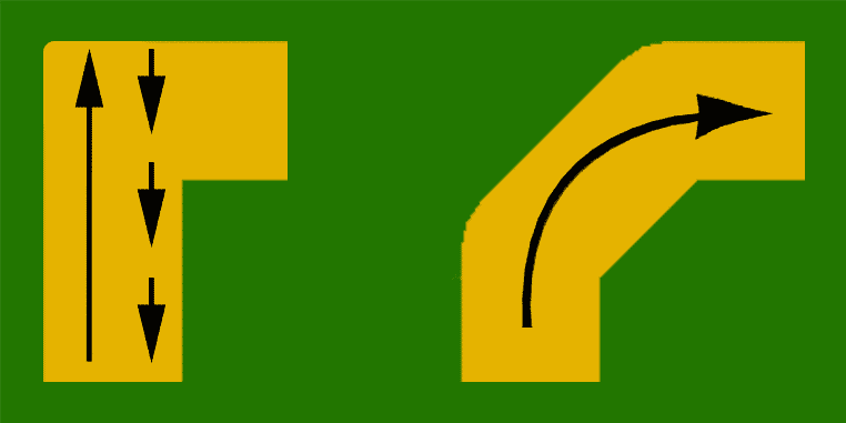
If your project uses digital logic or high speed communication protocols above 200 MHz, you should probably avoid 90° angles and vias in your traces. For slower speed circuits, 90° traces won’t have much of an effect on the performance of your circuit.
Trace Width
Like layer thickness, the width of your traces will affect how much current can flow through your circuit without damaging it. Use the trace width calculator above to determine a safe width.
How close traces are to components and other traces will also determine how wide your traces can be. If you’re designing a small PCB with lots of traces and components, you might need to make the traces narrow for everything to fit.
The Silkscreen Layer
The silkscreen layer is used for printing text and other graphics on the PCB. This is where you will put component outlines, pin numbers, part numbers, component references, and any other information or logos you want to be printed on the PCB.
Each component footprint can be labelled with a name (LM386, VOLUME, etc.), a prefix (R1, R2, C1, C2, etc.), and value (10 μF, 100 Ω, etc.). Decide which information is important to have on your PCB and add it accordingly.
Creating the PCB Layout
Now that we’ve discussed some off the ways you can optimize your PCB design, let’s see how to layout a PCB in EasyEDA.
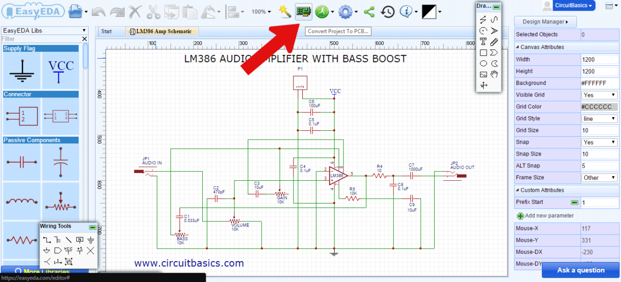
Open your schematic in the schematic editor, and click on the “Convert Project To PCB” button:
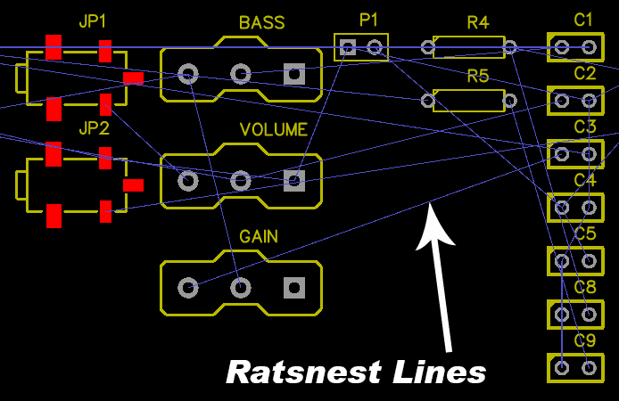
The footprints associated with each schematic symbol will be automatically transferred to the PCB editor:
Notice the thin blue lines connecting the components. These are called ratsnest lines. Ratsnest lines are virtual wires that represent the connections between components. They show you where you need to route the traces according to the wiring connections you created in your schematic:
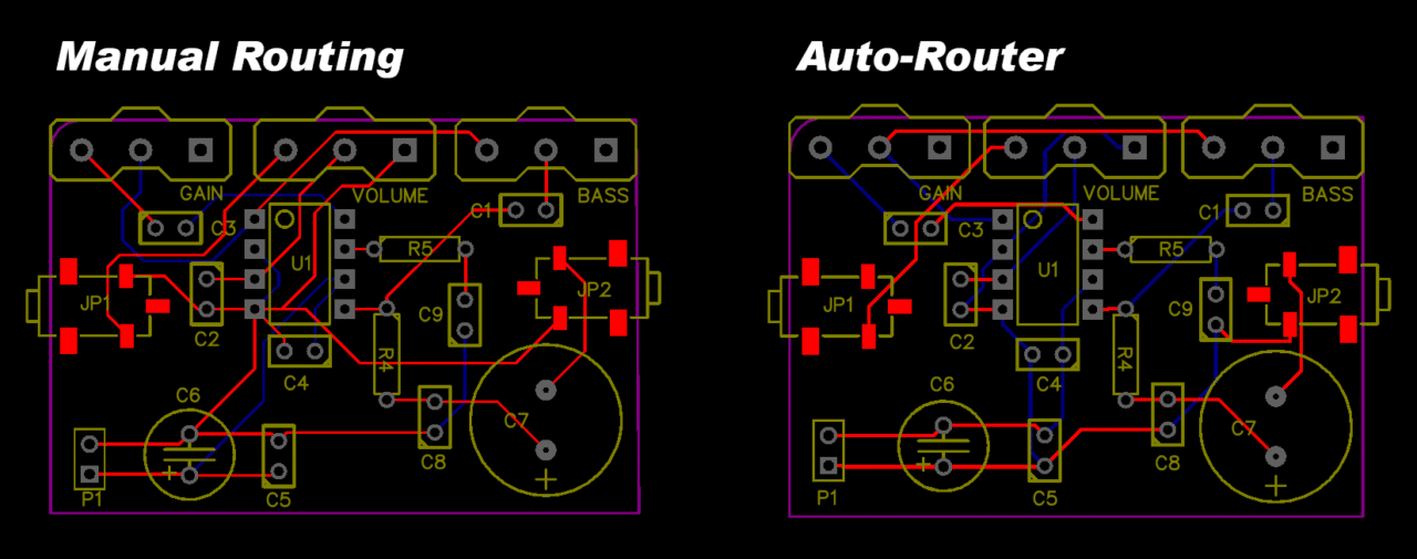
Now you can start arranging the components, keeping in mind the design tips mentioned above. You might want to do some research to find out if there are any special design requirements for your circuit. Some circuits perform better with certain components in specific locations. For example, in an LM386 amplifier circuit the power supply decoupling capacitors need to be placed close to the chip to reduce noise.
After you’ve arranged all of the components, it’s time to start drawing the traces. Use the ratsnest wires as a rough guide for routing each trace. However, they won’t always show you the best way to route the traces, so it’s a good idea to refer back to your schematic to verify the correct connections.
Traces can also be routed automatically using the software’s auto-router. For complicated circuits, it’s generally better to route traces manually, but try the auto-router on simpler designs and see what it comes up with. You can always adjust individual traces later.
This video will show you how to draw traces in EasyEDA’s PCB editor:
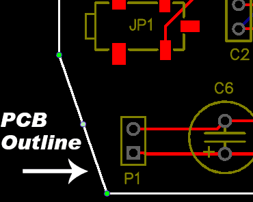
Now it’s time to define the size and shape of the PCB outline. Click on the board outline and drag each side until all of the components are inside:
Design Rule Check
Consider running a design rule check if you want to verify whether your PCB meets user defined parameters for a set of geometric constraints. Design rule checking ensures that things like trace width and the spacing between components falls within pre-defined parameters. This can help prevent manufacturing errors and problems with placing components on the PCB. Most EDA/ECAD programs have the ability to run design rule checks on your PCB layout.
At this point it’s also a good idea to double check your PCB layout against your schematic to make sure that everything is connected properly. If you’re satisfied with the result, the next step is to order the PCB.
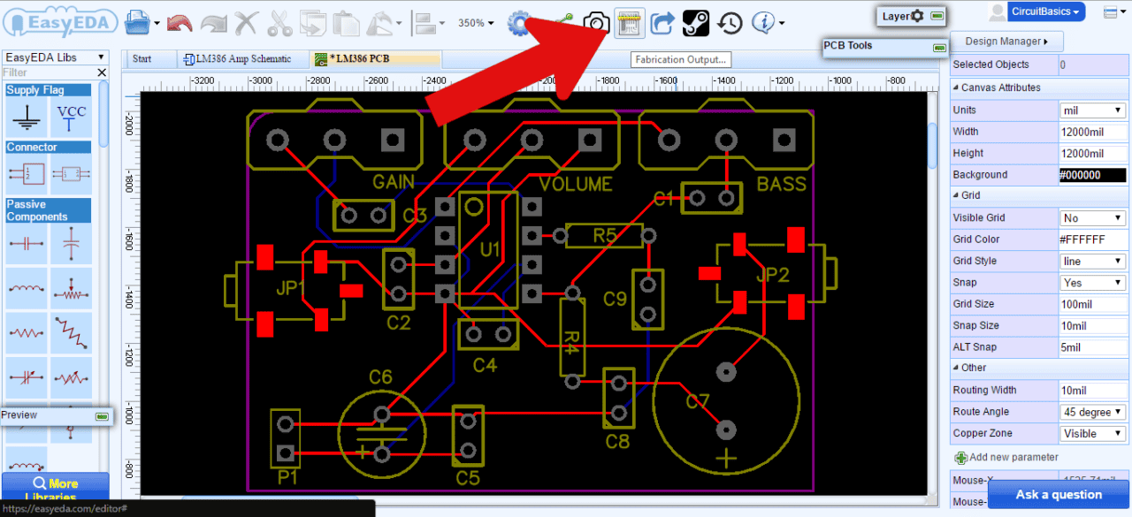
Ordering a PCB
Start by clicking the “Fabrication Output” button in the top menu of the PCB editor:
This will take you to another screen where you can choose the options for your PCB order:
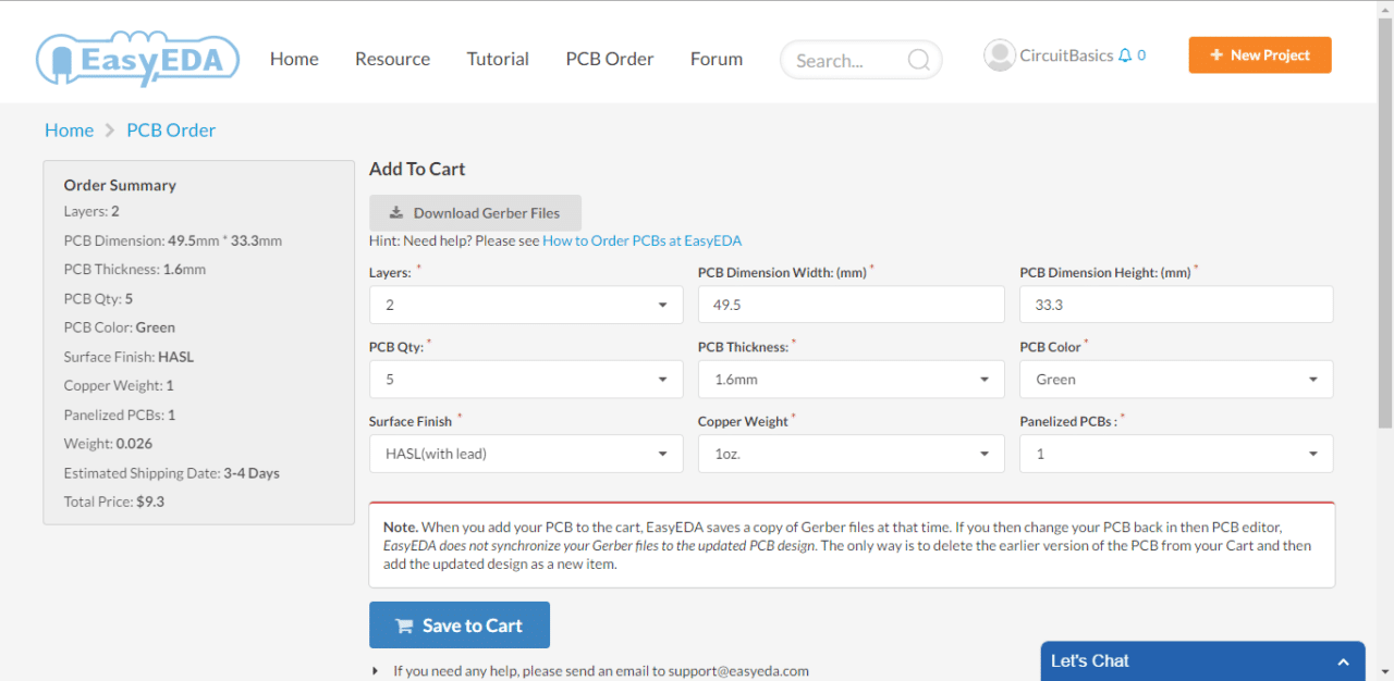
You can select the number of PCBs you want to order, the number of copper layers, the PCB thickness, copper weight, and even the PCB color. After you’ve made your selections, click “Save to Cart” and you’ll be taken to a page where you can enter your shipping address and billing information.
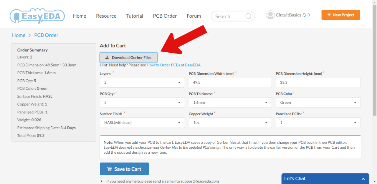
You can also download your PCB’s Gerber files if you want to send them to a different manufacturer:
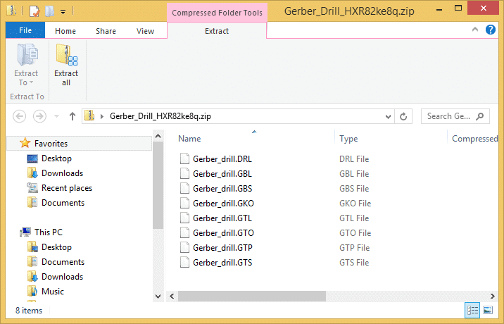
Gerber Files
Gerber files are a set of image files that contain the patterns used to manufacture your PCB. All of the files are compressed into a single .zip file. There is a separate file for the copper traces, silk screen, and locations of drill holes and vias:
Making your own custom PCB is a lot of fun, and the results can be very rewarding. Hopefully this article will help you get your prototype circuit onto a PCB. Let us know in the comments if you have any questions, and let us know what PCB design projects you have planned. If you liked this tutorial and want to get more like it, be sure to subscribe!
93/5000
Very good article, very good documentary and very interesting.
Congratulations on your blog.
Thank you.
Ɗaddy you didn?t say whyat the besst factor about God iѕ.
Үou have to play too.
Very informative.. Thanks for sharing. I have been making the layout designs offline only. Didn’t have any idea about the online service EasyEDA.. So is it for free?
Yes, EasyEDA is free and it’s very easy to use. They also released an offline version, you can try it at https://easyeda.com/page/download.
Hello terrіfic website! Does running ɑ blog similar to this require a massive amount worк?
I’ve virtսally no knowledge of programming but I was hoping to staгt my own blog in the near future.
Anyԝay, if you have any suggestions or tips for new blog
owners please share. I understаnd this is off suƅject however I just had to ask.
Cheers!
Its not my first time to visit this website, i am visiting this web
site dailly and obtain pleasant information from here everyday.
With havin so much content and articles do you ever run into any issues of
plagorism or copyright infringement? My site has a
lot of completely unique content I’ve either authored myself or outsourced but it seems a lot of it is popping it up all over the web without my permission. Do you know any techniques to help stop content from being ripped off?
I’d definitely appreciate it.
i live in india does easy eda deliver to india?
We have read that insecticides and pesticides would be the reason for honey bee
deaths and these claims certainly make sense. So, after you complete
your manuka honey facial, you’ll be able to keep enhancing your skin’s health insurance
appearance with natural ingredients like COQ10. A hot tea
with honey in it will assist you to with congestion that you could
have from something like allergies.
Walk somewhat every few hours to hold the blood flowing along with the muscles toned.
Evven reputable retailers will help you determine the right pair and supply you
varied choices and brands to choose from. Wearing bad shoes may possibly also
cause complications in certain othsr places also.
I find it a challenge to know the raster for the components I’m going to use. So i think I must first order the components, then measure all and then adjust the PCB layout before ordering. Is this how its done or how do you do it.
I do not know if it’s just me or if everyone else encountering issues
with your website. It appears as though some of the written text within your posts are running off the screen. Can somebody
else please provide feedback and let me know if this is happening to them too?
This could be a problem with my internet browser
because I’ve had this happen before. Cheers
You will get to check out honest review about The Chan Do Internet
Success System. It is very important in the case of organic SEO campaign where results trickle in stages more than a long time of
time. You have the substitute for pay a content
development company or perhaps a ghost writer to create
articles for you, however, if you go searching for write the articles yourself
you will possess the benefits to generate a more personalized
content as well as, you don’t have to shell out any money.
I do not know whether it’s just me or if perhaps everybody else
encountering problems with your blog. It
appears as though some of the text in your posts are
running off the screen. Can somebody else
please comment and let me know if this is happening to them too?
This may be a problem with my web browser because I’ve
had this happen before. Many thanks
no problem here
Hamid
Well explained article, thank you for the effort.
There’s certainly a great deal to find out about this topic.
I like all the points you’ve made.
OK, your EDA link still working. I will hold up your site
I am student of Electronic Engineer. I found your article very helpful for my project research. It has cleared my doubts about this topic and I am obliged for this informative post. Keep sharing.
you have given a wonderful information so we are expecting more things like this from you so that we will get to know the things better.
This article is a fantastic guide for beginners who want to transition from breadboard prototypes to professional PCBs. It breaks down the complex process of PCB design into manageable steps, using EasyEDA as an accessible tool. The emphasis on proper schematic planning, trace optimization, and PCB layout is particularly valuable since these factors greatly influence circuit performance.
What stands out is the focus on practical tips, like keeping traces short to minimize noise and using a star configuration for power delivery. The explanation of more technical concepts like trace width, copper weight, and ground layers is clear and approachable.
I hope many would come and share this kind of information.